Understanding Semiconductor Manufacturing
Semiconductor manufacturing is the foundation of modern electronics, powering everything from smartphones to complex industrial machinery. For business owners in the industrial and manufacturing sectors, understanding this intricate process and the pivotal role played by the photolithography machine can provide valuable insights into the capabilities and limitations of semiconductor manufacturing services.
The Semiconductor Manufacturing Process
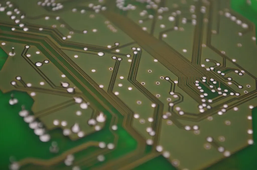
The semiconductor manufacturing process involves multiple sophisticated steps, each critical to the production of high-performance semiconductor devices. It starts with a silicon wafer, the base upon which millions of tiny circuits will be constructed. These circuits form the intricate pathways that allow electronic devices to function.
First, the wafer undergoes a series of preparatory steps, including cleaning and doping. Doping introduces impurities into the silicon wafer to alter its electrical properties. The doped wafer is then oxidized to create an insulating layer. Each step in the process must be executed with extreme precision to ensure the integrity and functionality of the final product.
Introduction to Photolithography
Photolithography plays a crucial role in defining the intricate patterns of circuits on the silicon wafer. This sophisticated technique involves using light to transfer a geometric pattern from a photomask to a light-sensitive chemical photoresist on the wafer. The photolithography machine, often referred to as the stepper or scanner, is at the heart of this process. It aligns and projects the photomask image onto the photoresist layer with sub-micrometer precision.
The photoresist undergoes chemical changes when exposed to light. Depending on whether a positive or negative photoresist is used, the exposed or unexposed regions will become soluble. Subsequent development steps remove the soluble areas, leaving a precise pattern of photoresist that mirrors the photomask design.
The Role of a Photolithography Machine
The photolithography machine controls several critical variables, such as the alignment of the photomask, the wavelength of the light source, and the exposure time. Advanced machines utilize deep ultraviolet (DUV) or extreme ultraviolet (EUV) light sources to achieve higher resolution patterns essential for modern semiconductor devices.
Alignment is a delicate process where the machine must position the wafer and photomask with nanometer precision. Any deviation can result in faulty circuits or reduced device performance. Automation and real-time monitoring systems integrated into modern photolithography machines ensure that the process is conducted with the necessary accuracy and consistency.
Exposure time is another crucial factor. It must be precisely controlled to ensure proper development of the photoresist pattern. Overexposure or underexposure can cause defects in the circuit pattern, leading to potential device failures. The photolithography machine’s ability to maintain consistent exposure times across multiple wafers is vital for large-scale semiconductor manufacturing.
The Importance of Photolithography in Semiconductor Manufacturing Services
The precision provided by photolithography directly impacts the performance, efficiency, and miniaturization of semiconductor devices. As devices become more complex and demand higher performance levels, the capabilities of photolithography machines must keep pace. This is particularly true in industries where semiconductors demand highly integrated and miniaturized components.
The evolving technology market continually pushes for smaller, faster, and more reliable semiconductor devices. Photolithography’s role becomes even more critical as it enables the production of devices with decreasing feature sizes, adhering to Moore’s Law. This law observes that the number of transistors on a microchip doubles approximately every two years, necessitating advanced photolithography techniques and machinery to maintain this trend.
Future Trends and Developments in Photolithography
Recent advancements in photolithography technology aim to overcome the limitations posed by traditional optical methods. For instance, EUV lithography represents a significant leap, allowing for even smaller feature sizes and higher precision levels. However, EUV lithography also presents challenges, such as the need for new materials, increased power requirements, and more sophisticated infrastructure.
Photolithography machines are central to semiconductor manufacturing, ensuring the precision and efficiency needed to produce modern electronic devices. To learn more about semiconductor manufacturing, contact us at Lithography Solutions.